

价格:5.00起
0
联系人:
电话:
地址:
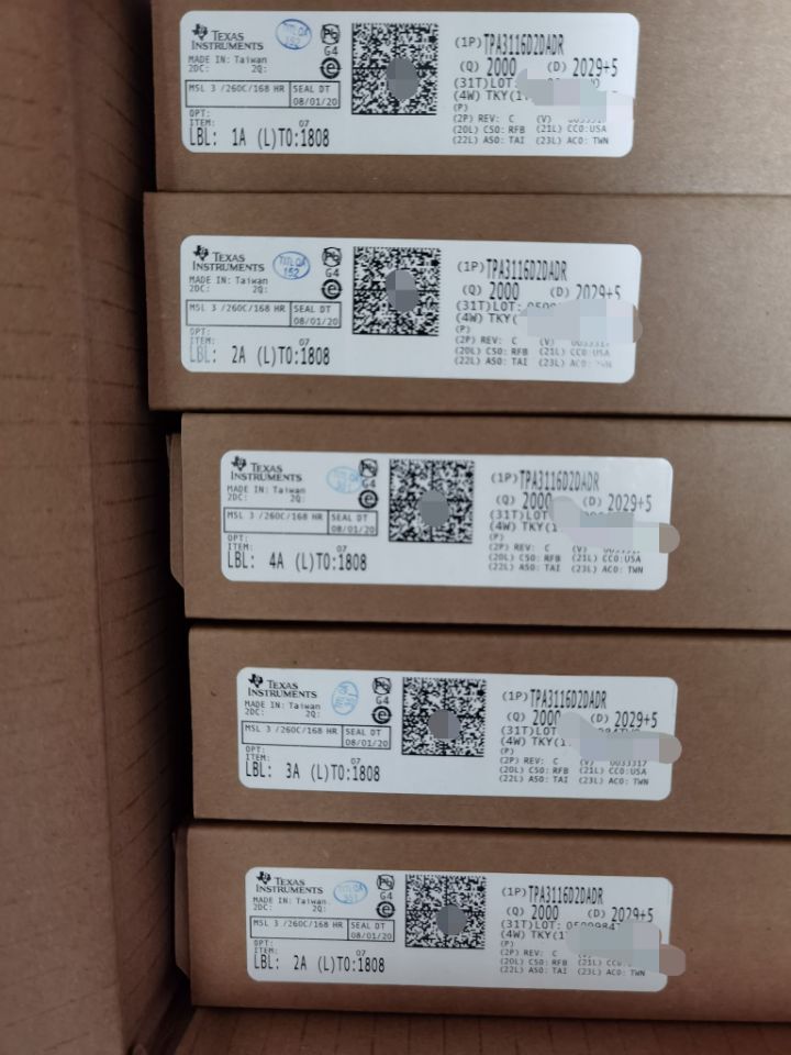
深圳市伟格兴电子科技有限公司是一家大型集成电路代理,分销商,公司在深圳.作为的集成电路分销商,我公司拥有丰富经验的IC销售人员,为客户提供全面的服务支持。我公司主要从事美国ADI、MAXIM,TI,ON,ST,FAIRCHILD,ADI,NXP等世界知名品牌的IC和功率模块 GTR、IGBT、IPM、PIM可控硅 整流桥 二极管等,涵盖通信、半导体、仪器仪表、航天航空、计算机及周边产品、消费类电子等广泛领域。公司现货多,价格合理。经过我公司全体人员的共同努力, 深圳市伟格兴电子科技有限公司现已成为国有大、中型企业,军工企业,中小型分销商的可靠合作伙伴,业务遍及中国大陆及海外市场。 我公司在国外拥有直接的货源和存货,与国际上享有良好声誉的大量供应商建立了良好的长期合作关系。定货渠道好,周期短,以‘交货快捷、质量保证、价格合理’为服务的宗旨,保证所提供货品均为原包装。 我公司一贯坚持:“品质、服务至上”的发展宗旨以向用户提供全方位系统 免费技术解决方案和满意的服务为己任。我们希望结交更多的合作伙伴,以合理的价格、全方位的服务,与大家共同开创广阔的未来!同时也希望与业界同行进行广泛的交流与合作,共同为电子业繁荣发展作出自己的贡献!7.5 Electrical Characteristicsover operating junction temperature (TJ = –40°C to 125°C), typical values at VIN = 12 V and TA=25°C (unless otherwise noted)PARAMETER TEST CONDITIONS MIN TYP MAX UNITSUPPLYVIN Input voltage range(1) 3 17 VIQ Operating quiescent current EN=High, IOUT = 0 mA,device not switching17 30µATA = -40°C to +85°C 17 25ISD Shutdown current(2) EN=Low1.5 25µATA = -40°C to +85°C 1.5 4VUVLO Undervoltage lockout thresholdFalling Input Voltage (PWM mode operation) 2.6 2.7 2.8 VHysteresis 200 mVTSD Thermal shutdown temperature 160°CThermal shutdown hysteresis 20CONTROL (EN, DEF, FSW, SS/TR, PG)VHHigh level input threshold voltage (EN,DEF, FSW) 0.9 0.65 VVL Low level input threshold voltage (EN,DEF, FSW)0.45 0.3 VILKG Input leakage current (EN, DEF, FSW) EN=VIN or GND; DEF, FSW=VOUT or GND 0.01 1 µAVTH_PG Power good threshold voltageRising (%VOUT) 92% 95% 98%Falling (%VOUT) 87% 90% 94%VOL_PG Power good output low IPG=–2mA 0.07 0.3 VILKG_PG Input leakage current (PG) VPG=1.8V 1 400 nAISS/TR SS/TR pin source current 2.3 2.5 2.7 µAPOWER SWITCHRDS(ON)High-side MOSFET ON-resistanceVIN≥6V 90 170mΩVIN=3V 120Low-side MOSFET ON-resistanceVIN≥6V 40 70mΩVIN=3V 50ILIMFHigh-side MOSFET forward currentlimit(3)VIN =12V, TA= 25°C3.6 4.2 4.9 AOUTPUTILKG_FB Input leakage current (FB) TPS62130, VFB=0.8V 1 100 nAVOUTOutput voltage range (TPS62130) VIN ≥ VOUT 0.9 6.0 VDEF (Output voltage programming) DEF=0 (GND) VOUTDEF=1 (VOUT) VOUT+5%Initial output voltage accuracy(4)PWM mode operation, VIN ≥ VOUT +1V 785.6 800 814.4mV PWM mode operation, VIN ≥ VOUT +1V,TA = –10°C to 85°C788.0 800 812.8Power Save Mode operation, COUT=22µF 781.6 800 822.4Tracking Feedback Voltage (TPS62130) VSS/TR = 350mV 212.6 225 237.4 mVLoad regulation(5) VIN=12V, VOUT=3.3V, PWM mode operation 0.05 %/ALine regulation(5) 3V ≤ VIN ≤ 17V, VOUT=3.3V, IOUT= 1A, PWMmode operation 0.02 %/VCUI Inc PDRB交流-直流DIN导轨电源CUI Inc PDRB交流-直流DIN导轨电源具有集成保险丝以及浪涌、过压和过流保护特性。这些电源提供多种选项,包括5W至300W的输出功率选项、5VDC至48VDC的输出电压选项以及螺钉或弹簧端子选项。特性集成保险丝和浪涌保护3,000Vac输入/输出隔离电压直流ON/LOW LED指示灯过压和过流保护弹簧和螺钉端子选项通过微调电位器 (Trim POT) 提供可调输出通过UL/cUL、TUV、CE认证规范输出电压选项:5VDC至48VDC输入电压:90Vac至264Vac隔离电压:3000Vac输出电流:0.21A至12.5A输出功率选项:5W至300W工作温度范围:-20°C至71°CThis integrated circuit can be damaged by ESD. Texas Instruments recommends that all integrated circuits be handled withappropriate precautions. Failure to observe proper handling and installation procedures can cause damage.ESD damage can range from subtle performance degradation to complete device failure. Precision integrated circuits may be moresusceptible to damage because very small parametric changes could cause the device not to meet its published specifications.DESCRIPTION (CONTINUED)Compared to the TPS65160 and TPS65160A the TPS65161/A/B family of devices offer increased step-downconverter output current. The TPS65161B also offers increased charge pump output current, and a higherundervoltage lockout threshold. The devices can be powered from a 12-V input supply and generate the fourmain supply voltages required by TFT LCD display panels.Each device comprises a boost converter to generate the source voltage VS, a step-down converter to generatethe logic supply V(LOGIC), and regulated positive and negative charge pumps to generate the TFT bias voltagesVGH and VGL. Both switching converters and both charge pumps operate from a central clock that can be set toeither 750-kHz or 500-kHz by tying the FREQ pin high or low.The TPS65161/A/B devices feature adjustable power supply sequencing, plus a number of safety features suchas boost converter overvoltage protection, buck converter short-circuit protection, and thermal shutdown. Thedevices also incorporate a gate drive signal to control an external MOSFET isolation switch connected in serieswith VS or VGH (see the application section at the end of this data sheet for more information).ORDERING INFORMATION (1)BOOST SWITCH CHARGE PUMP PACKAGE TA CURRENT LIMIT UVLO THRESHOLD ORDERING PACKAGE(3)CURRENT LIMIT (2) MARKING ILIM(min)2.8A 100mA 6V TPS65161PWP HTSSOP28 (PWP) TPS65161Table of Contents1 Features.................................................................. 1 7.4 Device Functional Modes........................................ 272 Applications ........................................................... 1 7.5 Programming........................................................... 357.6 Register Maps......................................................... 40 3 Description ............................................................. 18 Application and Implementation ........................ 48 4 Revision History..................................................... 28.1 Application Information............................................ 48 5 Pin Configuration and Functions......................... 38.2 Typical Applications ................................................ 49 6 Specifications......................................................... 58.3 System Examples ................................................... 52 6.1 Absolute Maximum Ratings ...................................... 59 Power Supply Recommendations...................... 53 6.2 ESD Ratings.............................................................. 59.1 LDO1 Output Voltage Adjustment........................... 53 6.3 Recommended Operating Conditions....................... 510 Layout................................................................... 53 6.4 Thermal Information.................................................. 610.1 Layout Guidelines ................................................. 53 6.5 Electrical Characteristics........................................... 610.2 Layout Example .................................................... 54 6.6 Battery Charger Electrical Characteristics ................ 96.7 Serial Interface Timing Requirements..................... 11 11 Device and Documentation Support ................. 556.8 Dissipation Ratings ................................................ 11 11.1 Third-Party Products Disclaimer ........................... 556.9 Typical Characteristics ............................................ 12 11.2 Community Resources.......................................... 5511.3 Trademarks ........................................................... 55 7 Detailed Description ............................................ 1711.4 Electrostatic Discharge Caution............................ 55 7.1 Overview ................................................................. 1711.5 Glossary ................................................................ 55 7.2 Functional Block Diagram ....................................... 187.3 Feature Description................................................. 19 12 Mechanical, Packaging, and OrderableInformation ........................................................... 55认准深圳伟格兴电子,地处亚太深圳。诚信13年合作伙伴。原装质量保证。只做原装现货!只做原装TI,DIODES,ON,NXP,ST,SKYWORKS,EALTEK ,RICHTEK 等国际知名品牌,产品线以单片机、逻辑、运放、驱动、存储、接口IC为主配单!优势现货渠道,如您刚好有需要,可别忘记找我这个老朋友问问


