

价格:10000起
0
联系人:
电话:
地址:
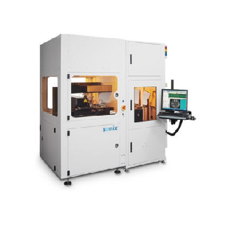
SONIX AutoWafer Pro™ 是专为全自动晶圆检测设计的机型,主要应用在Bond wafer,MEMS 内部空洞、离层检测,TSV量测方面。
● 使用于200和300mm晶圆
● 符合一级净化间标准
● Cassette装载,全自动检测,支持FOUP或FOSB机械臂
● 支持200mm & 300mm SECS/GEM协议
● KLARF输出文件
AutoWafer pro is our most advanced ultrasonic equipment for detecting defects in bonded wafers in a production environment, providing fast, high-resolution scanning of 200mm and 300mm bonded wafers.
A flexible, automated wafer inspection system designed for production, AutoWafer Pro provides fast, high-resolution scanning of 200mm and 300mm bonded wafers. It’s the ideal ultrasonic equipment for identifying bond defects in wafer applications such as MEMS, BSI Sensors, CMOS, memory, TSV and LED.
With extensive analysis capabilities at both the wafer and device level, there’s no need to reload and rescan wafers to get all the diagnostic images you need. And with high-speed scanning managed by fully automated wafer handling, AutoWafer Pro supports nondestructive testing (NDT) for improved yields and a faster time to market.


